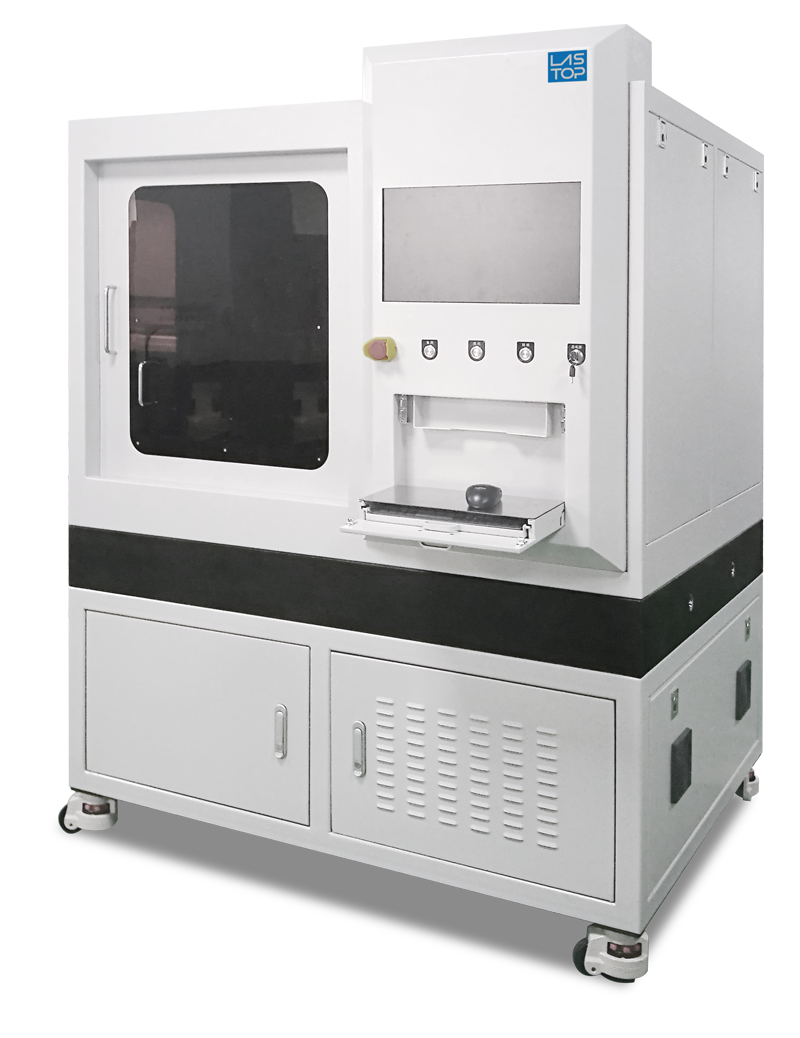
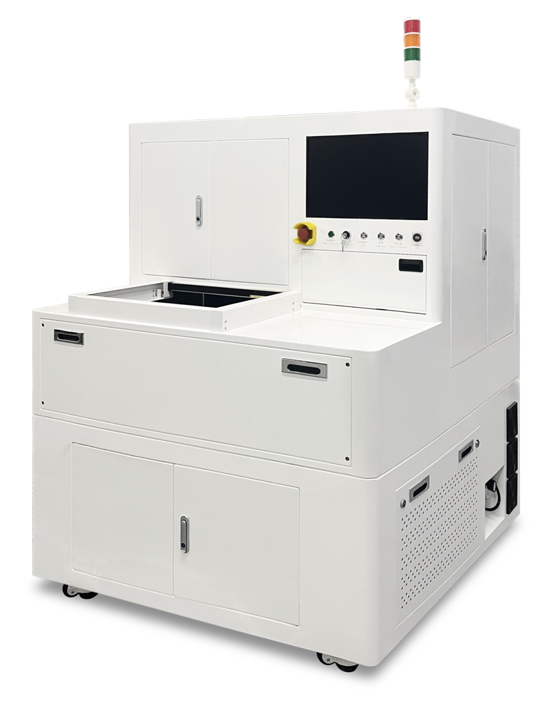
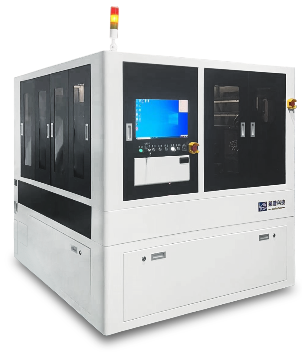
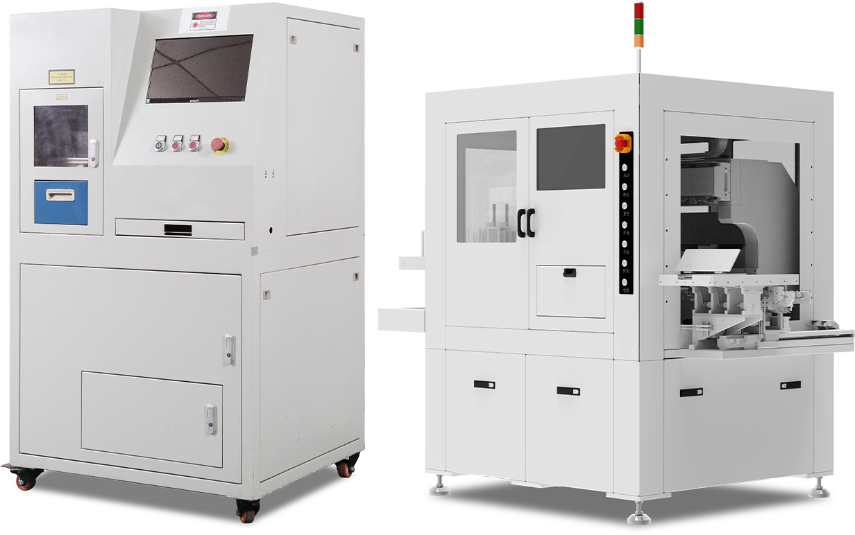
EN
Message Board
Send
Home
Products & Applications
Service & Support
About Us
Contact Us
PRECISION
ELECTRONICS
Laser Assisted
Bonding Welding | LAB
Application
Advanced Package Laser Assisted
Bonding, Mini/Micro LED
Laser Mega Welding
PCB X-OUT Laser
Marking | LM
Application
Automatic identification and laser marking
of scrap units after defect detection process
for semiconductor packaging boards and
electronic module boards
Automatic Substrate
Laser Marking | LM
Application
Fully automatic laser marking of
substrate products such as BGA/LGA/SIP
Ceramic Laser
Drilling/Dicing | LDR
Application
Precision drilling, cutting and
scribing of alumina/aluminium nitride/
zirconium oxide/silicon nitride,etc.
Glass Substrate
Laser Induced
Drilling | LDR
Application
Laser induced drilling through holes
and blind holes for special-shaped glass,
glass, RF components, optoelectronic
components, photomask plates, MEMS
components, glass based high-density
substrates, advanced wafer packaging,
glass spacer chips, Mini/Micro LED display
panel glass substrates, foldable screens, etc
Automatic Laser
Cutting | LC
Application
PCB/FPC/RF/Touch ID/Type-C/TF-Card/LGA/BGA
and other types of modules, circuit boards,
packaging IC carrier board precision cutting, slotting
PCB Module
Laser Cutting | LC
Application
PCB/FPC/RF/TouchID/Type-C/TF-Card/LGA/BGA
and other types of modules, circuit boards,
packaging IC carrier board precision cutting
and post-cutting inspection etc.
Dedicated laser
precision marking
equipment | LM
Application
Automatic laser labeling in the automotive
industry, cantilever laser marking in the auto
parts industry, laser engraving on calipers in
the gauging industry, large-format laser
marking in aviation and aerospace, automatic
marking in the PCB industry