Home
Products & Applications
Wafer Fabrication
Packaging & Testing
Precision Electronics
Service & Support
Service System
Industry Information
4 Hour Response
Provides Customization
And Transformation Services
Continuous
After-Sales Service
Sufficient Spare Parts
After-Sales Phone: 028-88556025
After-Sales Mail: lastop-service@la-ap.com
激光打标机的发展及趋势
激光器的应用与芯片切割工艺的现况
激光切割中的焦点位置检测方法研究
About Us
Company Profile
Company Culture
Development History
Company News
Honors
2003.12.23
2008.9
2012.1
2013.11
2021.7
2021.8.20
CSEAC2025圆满落幕 | 莱普科技获业界广泛关注!
莱普科技SEMICON China 2025:激光智造赋能半导体新未来
莱普科技惊艳亮相CSEAC2024
Culture
Business Philosophy
Corporate Culture
Quality Policy
Contact Us
Contact Us
Join Us
ADD: No.179 Kangqiang 3rd Rd, Gaoxin District,Chengdu, Sichuan, PR China
TEL: 028-88556027
Mail: lastop@la-ap.com
Wafer Fabrication: 028-85222347
Packaging&Testing: 028-88556026
Precision Electronics: 0755-23699089
Tel: 028-88556027
Mail: whx@la-ap.com
Latest recruitment positions: https://msearch.51job.com/jobs/all/co3240898.html
EN
中
Message Board
Send
中
EN
Home
Products & Applications
Wafer Fabrication
Packaging & Testing
Precision Electronics
Service & Support
Service System
Industry Information
About Us
Company Profile
Company Culture
Development History
Company News
Honors
Contact Us
Contact Us
Join Us
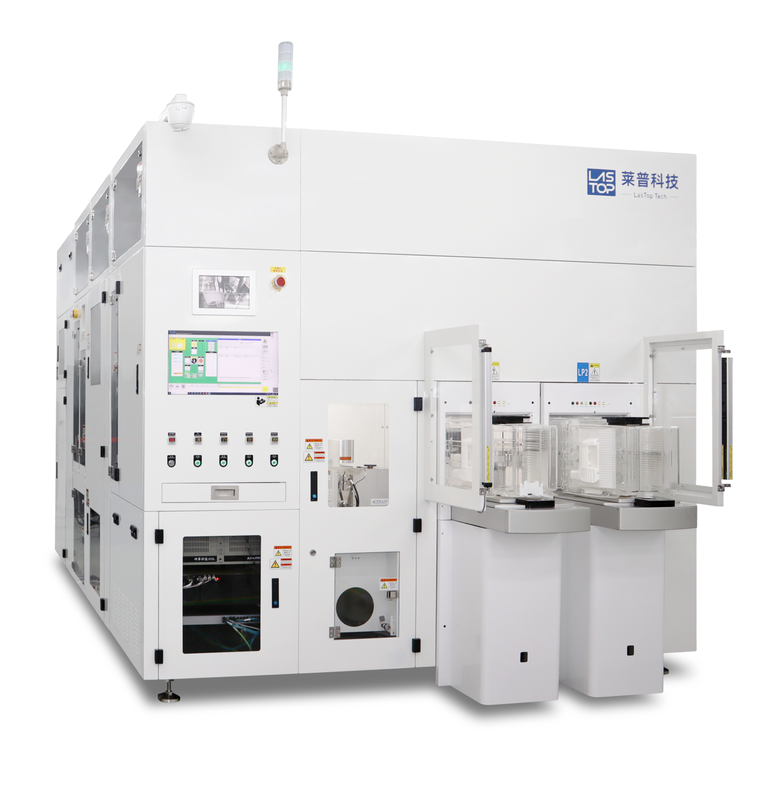
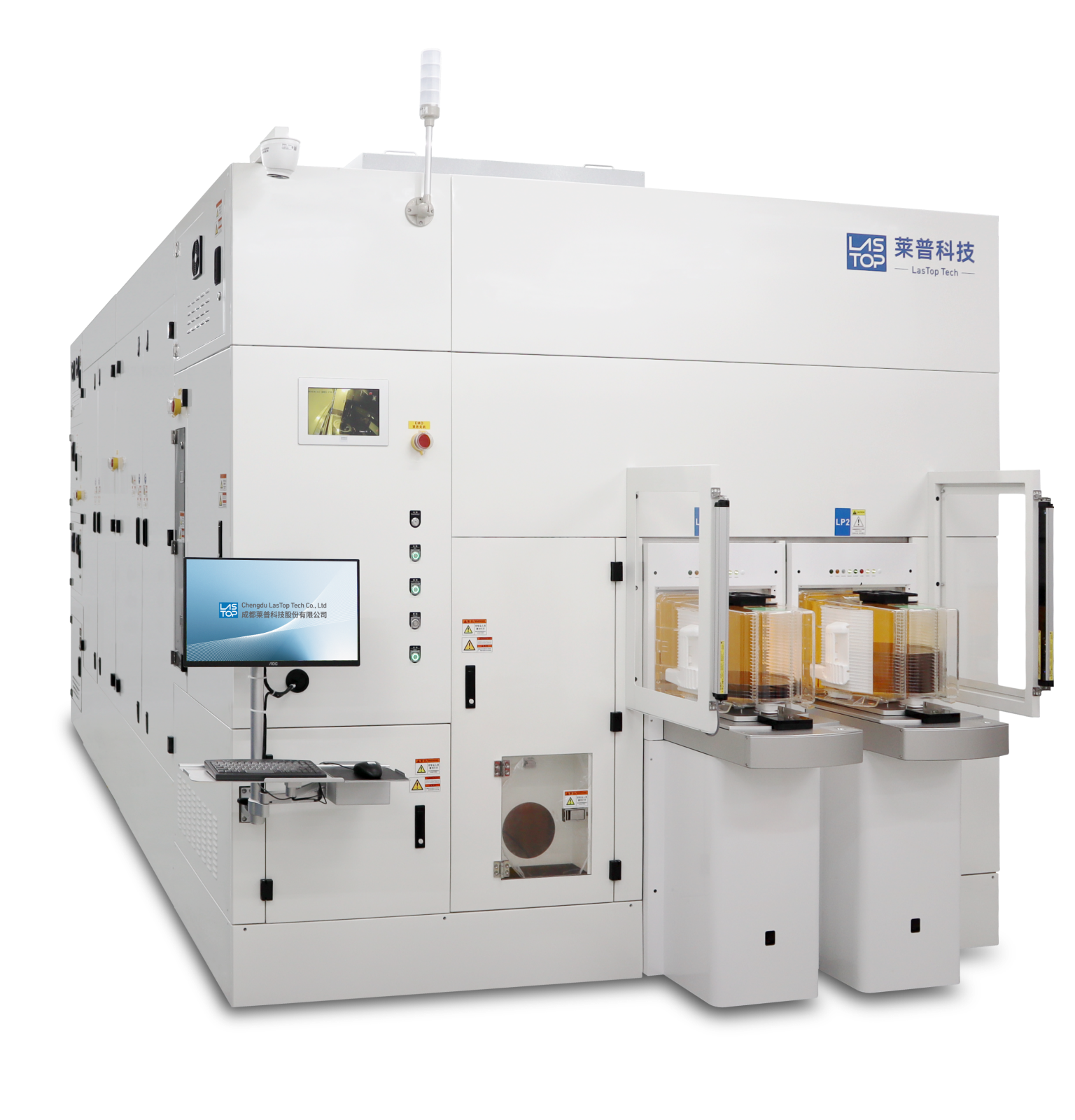
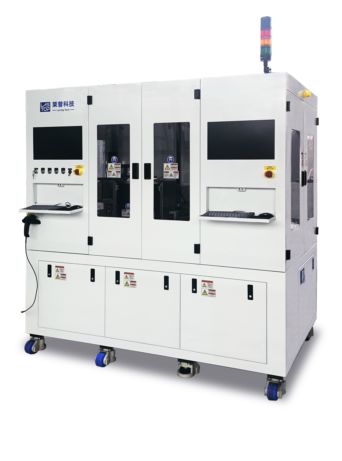
WAFER
FABRICATION
IGBT
Laser Annealing
| LA
Application
Ion-activation for silicon IGBT
SiC
Laser Annealing
| LA
Application
Ohmic contact preparation for SiC wafers
Laser Induced
Crystallization | LIC
Application
Laser crystallization
and in-situ dopant activation of
amorphous materials
Laser Induced
Epitaxial Growth | LIEG
Application
Laser-induced epitaxial growth and
void elimination of amorphous silicon in
ultra-small via with large aspect ratio
Ultra-shallow
dopant laser annealing | LA
Application
Ultra-shallow dopant laser
annealing for BSI-CCD wafer
Wafer Laser
Marking | WLM
Application
Si wafer, Bonded wafer,
SiC/Saphire wafer laser marking
PRODUCTS & APPLICATIONS
Wafer Fabrication
Packaging & Testing
Precision Electronics